← Cinco de Mayo Coloring Pages for Toddlers: Safe Cinco de mayo coloring pages mexican fiesta cinco de mayo coloringcinco Wiring Diagram for Beginners: Master the Basics in One Weekend How to read car wiring diagrams for beginners →
If you are looking for Standard PCB Thickness - Determine the Right Standards you've visit to the right place. We have 25 Pictures about Standard PCB Thickness - Determine the Right Standards like Detailed Procedures of Plating Copper for PCB Processing - PCB, Detailed Procedures of Plating Copper for PCB Processing - PCB and also PCB manufacturing Process & Equipment - PCBWay. Here it is:
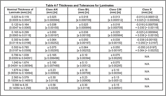
Standard PCB Thickness - Determine The Right Standards
 www.ourpcb.com
Standard PCB Thickness - Determine the Right Standards
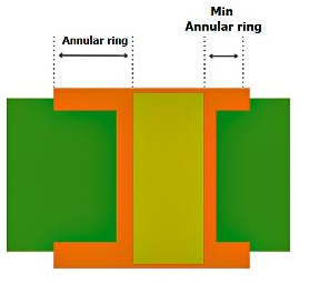
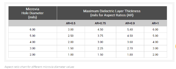
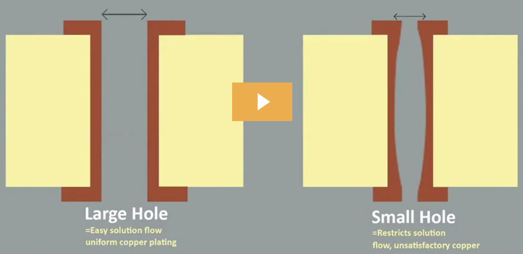
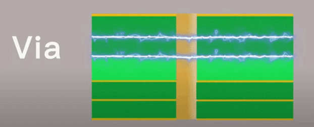
The Ultimate Guide To Understanding Via Plating Thickness In PCBs - Top
 camtechpcb.com
The Ultimate Guide to Understanding Via Plating Thickness in PCBs - Top ...
The Ultimate Guide To Understanding Via Plating Thickness In PCBs - Top
 camtechpcb.com
The Ultimate Guide to Understanding Via Plating Thickness in PCBs - Top ...
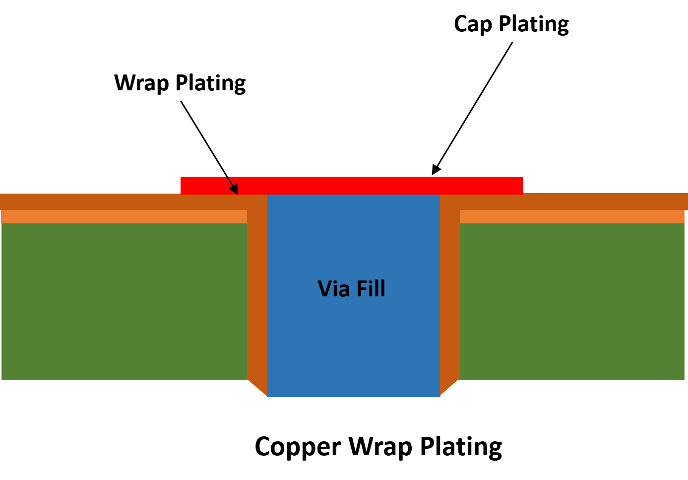
Copper Wrap Plating For PCB Manufacturing | Sierra Circuits
 www.protoexpress.com
Copper Wrap Plating for PCB Manufacturing | Sierra Circuits
PCB Via Plating: Depth Guide And Process - Jhdpcb
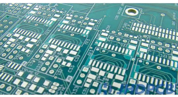 jhdpcb.com
PCB Via Plating: Depth Guide And Process - Jhdpcb
The Ultimate Guide To Understanding Via Plating Thickness In PCBs - Top
 camtechpcb.com
The Ultimate Guide to Understanding Via Plating Thickness in PCBs - Top ...
Inspirasi Pcbway Via Plating Thickness, Skema Pcb
 skemadriver.blogspot.com
Inspirasi Pcbway Via Plating Thickness, Skema Pcb
The Ultimate Guide To Understanding Via Plating Thickness In PCBs - Top
 camtechpcb.com
The Ultimate Guide to Understanding Via Plating Thickness in PCBs - Top ...
Inspirasi Pcbway Via Plating Thickness, Skema Pcb
 skemadriver.blogspot.com
Inspirasi Pcbway Via Plating Thickness, Skema Pcb
Inspirasi Pcbway Via Plating Thickness, Skema Pcb
 skemadriver.blogspot.com
Inspirasi Pcbway Via Plating Thickness, Skema Pcb
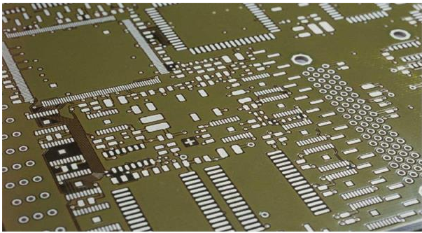
Detailed Procedures Of Plating Copper For PCB Processing - PCB
 www.pcbway.com
Detailed Procedures of Plating Copper for PCB Processing - PCB ...
The Ultimate Guide To Understanding Via Plating Thickness In PCBs - Top
 camtechpcb.com
The Ultimate Guide to Understanding Via Plating Thickness in PCBs - Top ...
Plating Thickness Under Different Plating Time | Download Scientific
 www.researchgate.net
Plating thickness under different plating time | Download Scientific ...
Detailed Procedures Of Plating Copper For PCB Processing - PCB
 www.pcbway.com
Detailed Procedures of Plating Copper for PCB Processing - PCB ...
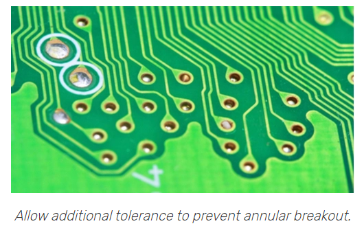
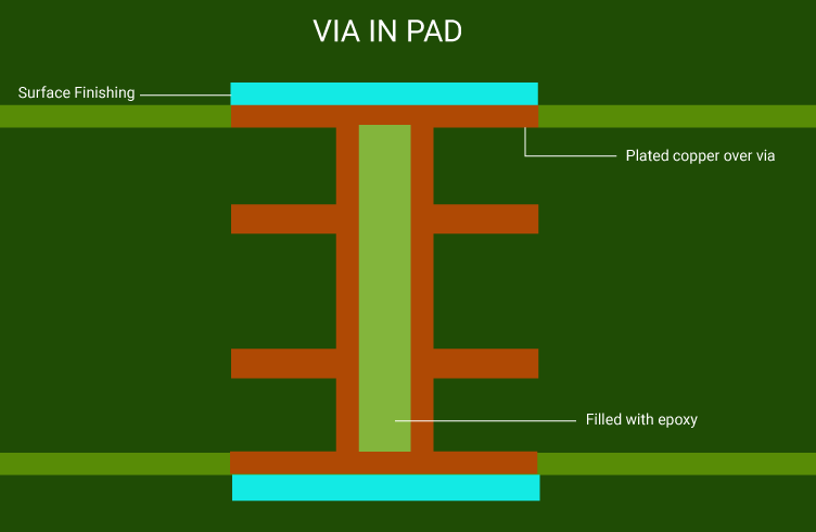
Via-in-Pad In PCB Design Manufacturing | Sierra Circuits
 www.protoexpress.com
Via-in-Pad in PCB Design Manufacturing | Sierra Circuits
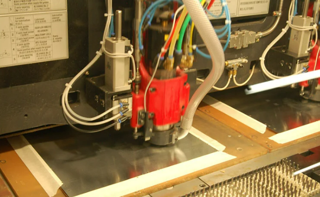
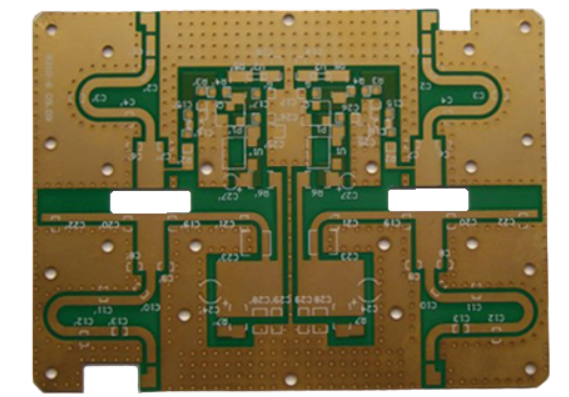
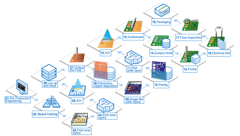
PCB Manufacturing Process & Equipment - PCBWay
 www.pcbway.com
PCB manufacturing Process & Equipment - PCBWay
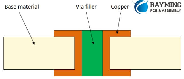
Via-filling Plating In PCB Manufacturing Process
 www.raypcb.com
Via-filling Plating in PCB Manufacturing Process
The Ultimate Guide To Understanding Via Plating Thickness In PCBs - Top
 camtechpcb.com
The Ultimate Guide to Understanding Via Plating Thickness in PCBs - Top ...
Why Some PCBs Need Edge Plating? - Technology - PCBway
 www.pcbway.com
Why Some PCBs Need Edge Plating? - Technology - PCBway
The Ultimate Guide To Understanding Via Plating Thickness In PCBs - Top
 camtechpcb.com
The Ultimate Guide to Understanding Via Plating Thickness in PCBs - Top ...
The Ultimate Guide To Understanding Via Plating Thickness In PCBs - Top
 camtechpcb.com
The Ultimate Guide to Understanding Via Plating Thickness in PCBs - Top ...
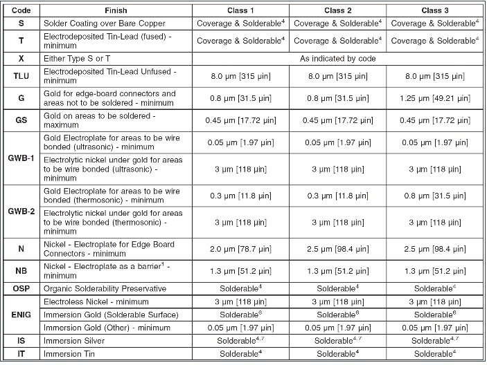
IPC Standards For Surface Plating
 www.sharedpcb.com
IPC Standards for Surface Plating
The Ultimate Guide To Understanding Via Plating Thickness In PCBs - Top
 camtechpcb.com
The Ultimate Guide to Understanding Via Plating Thickness in PCBs - Top ...
PCB Edge Plating - A Complete Guide - IBE Electronics
 www.pcbaaa.com
PCB edge plating - a complete guide - IBE Electronics
Inspirasi Pcbway Via Plating Thickness, Skema Pcb
 skemadriver.blogspot.com
Inspirasi Pcbway Via Plating Thickness, Skema Pcb
The ultimate guide to understanding via plating thickness in pcbs. Why some pcbs need edge plating?. Inspirasi pcbway via plating thickness, skema pcb